

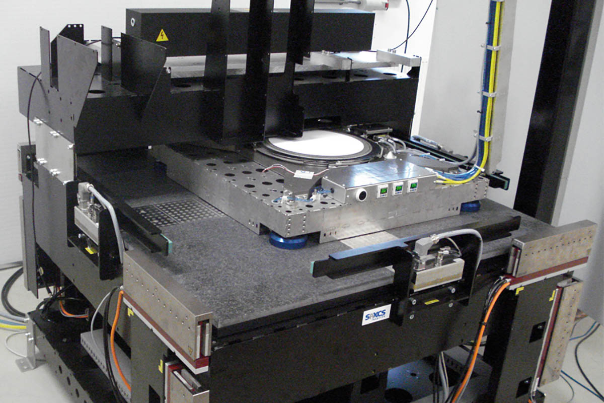
Subject to tremendous market pressure, ASM PT needed to engineer its disruptive technology prototype towards commercial release: a fully automated 12” wafer dicer with extremely high position and grooving/dicing accuracy (< ± 1µm) in a small footprint. Sioux was asked to help develop the Advanced Laser-Induced Subsurface Separation (ALISS) in collaboration with VDL ETG.
Sioux acted as the main contractor. Mechanics, mechatronics, optics, electronics and software design were performed in-house. Five new mechatronic modules were added to the prototype 12’ control software (Thor). Changes were made in all layers of the Thor architecture (the I/O layer, the System layer and the Control/Application layer): wafer height mapping, recipe parsing and dicing trajectory calculation, contour mapping, wafer alignment using on- and off-axis cameras and laser control application.
With this new machine, ASM PT is able to offer laser dicing and grooving systems that ensure the lowest possible cost of ownership due to the shortest possible process time (keeping up cutting speeds of up to 500mm/s) and offer high flexibility.
Computer Vision, Sensor processing, C++, VCL, Python, TCP/IP, Machine dynamics and planar XY stage.
ASM PT is the inventor of laser dicing and the world’s leading provider of laser-dicing systems for the semiconductor industry. The process is based on unique multi-beam laser-dicing technology with very low thermal impact and very high productivity.
